ADVANCED MANUFACTURING & SENSING
The Advanced Manufacturing and Sensing (AMS) program seeks to understand the fundamental limits and application of additive manufacturing technologies, devices for Beyond Moore’s computing, next-generation optical and RF communication systems, sensing platforms, and hardware trust. Our laboratory facilities house state-of-the-art nanoscale device fabrication and packaging capabilities. We partner with leading academic, industrial, and governmental research organizations to assure that our customers have access to the most advanced research developments and scientific insights.
ADVANCED MATERIALS
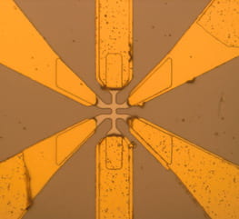
We utilize state-of-the-art fabrication and characterization facilities to develop novel materials and devices with great promise for emerging memory, logic, and sensing applications. In order to determine which materials to incorporate in advanced memory and logic devices, these new materials are integrated with novel devices structures for advanced testing to determine benefits and limitations. LPS provides unique measurement capabilities that are leveraged by partners throughout the community.
ADDITIVE MANUFACTURING
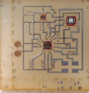
We research and develop the fabrication and rapid prototyping of novel electronic components and systems utilizing advanced additive manufacturing technologies. Areas of research include materials characterization, printed interconnects, antennas and RF components, printing platforms, embedded components for replacing surface mount components, and novel substrates such as textiles.
INTEGRATED PHOTONICS
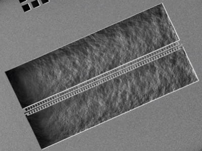
We develop special purpose photonic integrated circuits (PICs) for sensing and high-speed communications. Hybrid Silicon photonics have a distinct advantage over other platforms by combining both the active and passive components required for a multitude of devices needed for high-speed optical communications, data center interconnects, and microwave photonics. LPS aims to bring together technical expertise from government and academic researchers to make fundamental breakthroughs in the field of integrated photonics by researching low size, weight, and power (SWAP) solutions for future optical communication challenges and to address the ever-increasing bandwidth demands for future applications.
HARDWARE TRUST
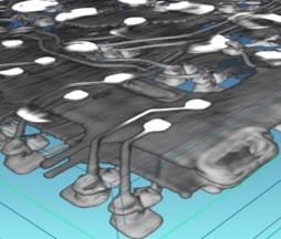
We research novel imaging techniques to facilitate the failure analysis and characterization of traditional and additively manufactured devices and electronics, supporting research areas across the LPS. Imaging equipment includes scanning electron, atomic force, and computed tomography x-ray microscopes.
ELECTROMAGNETICS & ADVANCED ANTENNA DESIGN
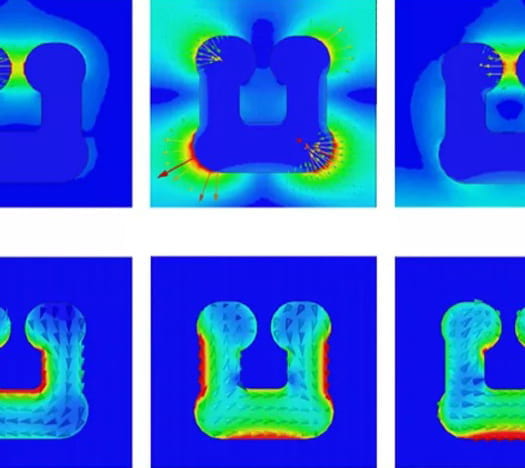
We study new materials, tools, and approaches to improve the performance of electromagnetic systems, components, and devices. Areas of research include sensor systems, advanced antenna modulation, improving bandwidth and radiation efficiency, beam steering, antenna miniaturization, and low profile antennas. LPS directly engages with the research community to advance unique needs in antenna and E&M system development.

